
Transmission and scanning transmission electron microscopy (TEM/STEM)
Compared to light and scanning electron microscopy transmission electron microscopy (TEM) achieves a significantly enhanced spatial resolution. Thanks to the small wavelength of the electrons in the TEM feature sizes of the order of 0.1 nm are resolved.
Conventional TEM
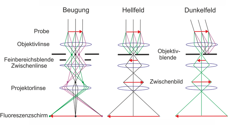

Owing to the interaction with the atoms the incident electrons experience a deflection inside the object corresponding to a phase shift in the wave picture. This deflection depends on the atomic number and of the number of atoms passed (mass thickness contrast). In case of crystalline objects also diffraction contrast occurs, i.e. the scattered intensity is a function of the crystal orientation relative to the electron beam. The undiffracted or diffracted beams used for bright field or dark field imaging are selected by means of a diaphragm in the back focal plane of the objektive lens. Hereby the structural information extracted from the diffraction pattern can be assigned to tiny regions in the specimen. Conventional TEM permits imaging of the morphology, the spatial distribution of chemical-crystallographic phases as well as of lattice defects in material structures.
Electron diffraction
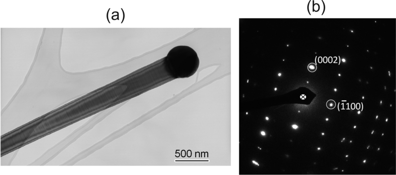
Electron diffraction patterns form due to the interference of the electron wave at the lattice planes of crystalline objects. In case of parallel illumination (selected area diffraction, SAED) diffraction spots are obtained in the back focal plane of the objective lens, whereas in case of convergent illumination discs are formed, whose diameters depend on the convergence angle. In selected area diffraction specimen areas of minimum size ~0.1 µm can be selected by means of a diaphragm. Convergent illumination using a (partially) focused beam permits to analyze specimen areas with size < 5 nm.
Selected area diffraction is employed for phase and texture analysis on a sub-micrometre length scale. In addition phase transitions can be studied with temporal resolution in thermal or mechanical in-situ experiments. Convergent electron diffraction is used for the highly precise, spatially resolved determination of lattice parameters.
High-resolution TEM (HRTEM)
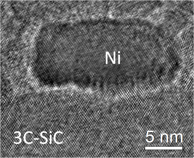
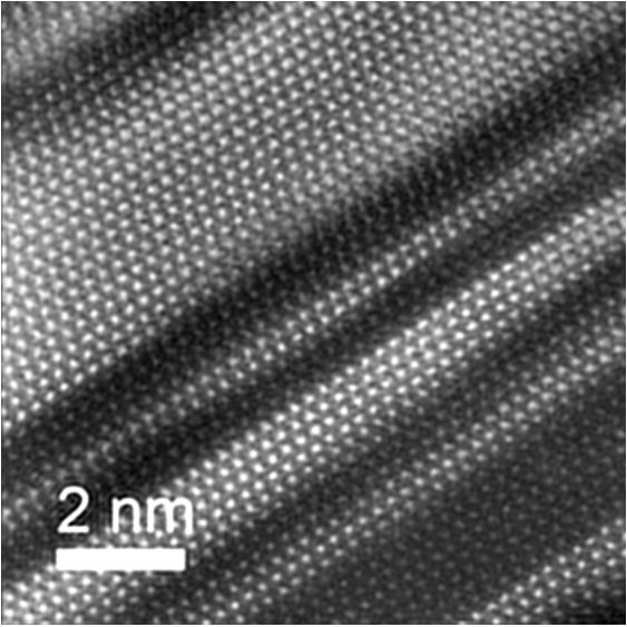
In crystalline objects the electron wave experiences phase shifts, which reflect the periodic arrangement of the atoms in the crystal lattice (phase contrast). Therefore, the high-resolution image represents a projection of the crystal lattice, folded with the contrast transfer properties of the microscope. For a correct image interpretation various parameters such as defocus, specimen thickness and aberrations of the magnetic lenses have to be considered.
HRTEM imaging enables atomically resolved characterisation of the structure of lattice defects like dislocations or interfaces.
Scanning transmission electron microscopy (STEM)
In contrast to conventional and high-resolution TEM in STEM mode the image is sequentially recorded using a finely focussed electron beam, which scans the object line per line. Similar to conventional TEM the intensity distribution in STEM bright field images is governed by the mass thickness and diffraction contrast mechanisms. Here the electrons scattered in forward direction are registered on a detector.
If instead those electrons are detected that have been incoherently scattered under large angles, dark field images are obtained, whose contrast is dominated by differences of the mean atomic number, so-called high-angle annular dark-field STEM (HAADF-STEM) or Z-contrast images. This method allows to image local variations of the chemical composition on the nanometer scale. Given a high mechanical stability of the specimen lattice images can dbe directly interpreted, thanks to the high degree of information localisation. Combined with energy-dispersive X-ray spectroscopy and electron energy-loss spectroscopy STEM enables quantitative analyses of the composition and the electronic structure at atomic resolution.
Energy filtered TEM (EFTEM)
In energy filtered TEM electrons of a selectable energy loss region are used for the image or the diffraction pattern. This is realized with an imaging energy filter, which is attached to the bottom edge of the TEM column or alternatively inserted into the imaging system. EFTEM is suitable for various applications, such as:
- Improvement of contrast and resolution in conventional and high-resolution TEM images by means of removal of the inelastically scattered electrons
- Extended structural information extracted from elastically filtered diffraction patterns
- Imaging of the spatial distribution of plasmonic excitations, elemental composition, bonding states and TEM foil thickness
Author: Dr. Thomas Riedl