Periodic poling
Already Armstrong et al. [1] pointed out that a periodic inversion of the sign of χ(2) can compensate for a phase mismatch between driving nonlinear polarization and the driven electromagnetic waves during three wave mixing, called quasi-phase matching. For our ferroelectric waveguide substrates the sign of χ(2) coefficients is related to the orientation of the spontaneous polarization. Therefore, a periodic change of the sign of χ(2) , a χ(2) grating, can be created by a periodic inversion of the spontaneous polarization, also called periodic poling [2].
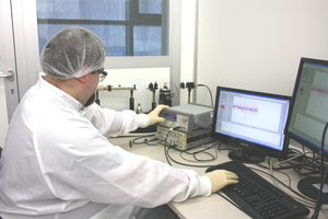
Lithium niobate substrates can be periodically poled in our cleanroom facility using the standard field assisted poling technique with a monitor for the accumulated charge. Like structuring the waveguides, a photoresist is spin-coated to the sample’s surface, followed by the illumination through a specific mask. After development the properly baked resist structure acts as electrical insulation during the poling process whereas non-covered regions are contacted using a LiCl-solution as liquid electrode. We subsequently apply high voltage pulses to overcome the coercitive field strength of about 22 kV/mm. This technique allows for the realization of periodicities down to ΛG ~ 4 μm. The steps necessary for periodic poling are schematically shown in Fig 1.
For poling of the KTP-substrates control of the process by monitoring the accumulated charge does not work, due to the ionic conductivity of KTP. We therefore apply an optical monitoring technique as developed by Canalias et al. [3].
Because of the strong distortion of the crystal lattices during the poling procedure the samples must be annealed for several hours at temperatures in the range 250 − 400°C. This reduces stress-induced refractive index changes at the domain interfaces and the associated scattering losses in the waveguide.
We subsequently clamp the samples into a special holder filled with an electrolytic agent and apply high voltage pulses to overcome the coercitive field strength of about 22kV/mm. By applying this voltage the spontaneous polarization in the contacted areas changes its sign after the correct amount of conducted charge.
Because of the strong distortion of the crystal lattices during the poling procedure the samples must be exposed to an annealing process at 400°C for at least two hours. This reduces stress and strain at the domain interfaces and provides us with low scattering losses in the waveguide.
References
- Interactions between light waves in a nonlinear dielectric
J. A. Armstrong, N. Bloembergen, J. Ducuing, and P. S. Pershan
Physical Review, 127(6):1918–1939, September 1962 - First-order quasi-phase matched LiNbO3 waveguide periodically poled by applying an external field for efficient blue second-harmonic generation
M. Yamada, N. Nada, M. Saitoh, and K. Watanabe
Applied Physics Letters, 62(5):435–436, February 1993 - Periodic poling of KTiOPO4: From micrometer to sub-micrometer domain gratings
C. Canalias, V. Pasiskevicius, and F. Laurell
Ferroelectrics, 340(1):27–47, 2006


