
Research & Facilities
The group of Optoelectronic Materials and Devices at the University of Paderborn focuses its research on the fabrication and characterization of semiconductor heterostructures for optical and electronic applications, for instance in quantum-information technology.
In these semiconductor heterostructures quantum effects are employed in order to realize new properties. Atomically sharp energy levels in semiconductor quantum dots are one example.
One major focus of our work is the fabrication of semiconductor heterostructures by molecular beam epitaxy (MBE), an ultra-high-vacuum deposition process that allows highest material quality as well as highest material purity. After growth, these heterostructures are analyzed structurally, optically and electrically. For structural examination high-resolution x-ray diffraction, scanning and transmission electron microscopy as well as atomic force microscopy is used.The samples are optically characterized by photoluminescence spectroscopy and reflectivity measurements. The experiments can be performed at room temperature as well as at low temperatures.
For electrical characterization mainly Hall-effect measurements, capacitance voltage spectroscopy and current-voltage measurements are employed. Seminconductor heterostructures are partly further processed into basic devices whereby modern patterning processes, for example electron beam lithography and reactive ion etching (RIE), are used. A special feature of the work group are the different semiconductor material systems, which cover the wide spectral range from infrared to ultraviolet light.
In detail, we produce heterostructures on the basis of the following semiconductor systems:
Group III-Arsenides and Antimonides (Prof. Dr. Dirk Reuter)
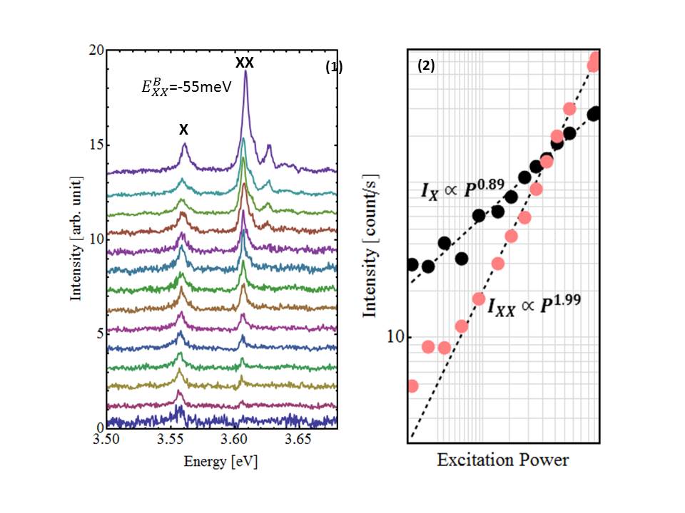
The group III- arsenides (InAs, GaAs, AIAs) cover the spectral range of about 0,7 to 1,3 µm.
The corresponding antimonides allow for expanding the spectral range down to 3 µm and also make the wavelength of 1,55 µm accessible, which is vital for fiber-bound communication.
All in all the InAs/GaAs/AIAs-system allows not only for the fabrication of highest quality layered structures in the AlAs/GaAs-sub-system but also for the realization of semiconductor quantum dots of excellent optical qualities the InAs/GaAs-sub-system. Overall this system enables the fabrication of quantum dot heterostructures of finest material quality.
One focus of our activities is the fabrication of InAs quantum dot-structures for quantum dot information technology, for instance to implement single photon sources or exciton qubits.
In the field of single photon emitters and detectors we develop new device concepts, with one focus on 1,55 µm operational wavelength.
By embedding InAs quantum dots into special heterostructures, the charge in the quantum dots or the emission wavelength can be adjusted by an external electrical voltage.
Furthermore we deal with the MBE on pre-patterned substrates to fabricate complex quantum devices.
Cubic goup III nitrides (Apl. Prof. Donat As)
Group III nitrides like GaN, AIN, und InN are, due to their mechanical strength/stability and chemical and thermal resistance, particularly suitable for electronic (transistors) and optoelectronic applications like blue light emitting diode laser, which work at extreme environmental conditions and high frequencies.
For devices of structure sizes in the nanometer range new qualities and effects become obvious which can for example be used for single photons or THz emitters, respectively detectors.
The main field of research of our specialist area, integrated in the Center of Optoelectronics and Photonics Paderborn (CeOPP), is the fabrication of cubic group III nitrides with molecular beam epitaxy and its characterization by optical, electrical and structural measuring techniques, as well as the production of first device structures.
These works on the basis of cubic III-nitrides led to the realization of the first field effect transistor of cubic AIGaN/GaN, as to quantum dot emitters and inter-subband quantum-well photo-detectors (QWIPs). For the first time single photon emissions of cubic quantum dots up to 200 K were proved just recently.