
A warm welcome!
The group for optoelectronic materials and devices deals with the production and characterisation of semiconductor structures for optical and electronic applications, e.g. in quantum information technology. Quantum effects are utilised in these semiconductor structures in order to obtain novel properties. One example of this is the atomically sharp energy levels in semiconductor quantum dots.
Research
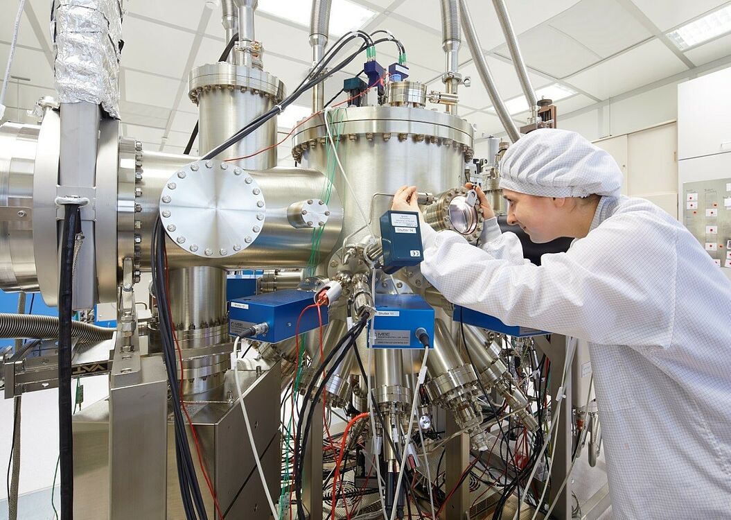
One focus of our work is the production of semiconductor heterostructures using molecular beam epitaxy (MBE), an ultra-high vacuum deposition process that enables the highest material qualities and purities. After growth, these heterostructures are characterised structurally, optically and electrically. For structural analyses, we use high-resolution X-ray diffraction, scanning and transmission electron microscopy and atomic force microscopy. Optically, the samples are analysed using photoluminescence spectroscopy, reflection measurements and spatial resolution methods. Electrical characterisation is mainly carried out using Hall measurements, capacitance-voltage spectroscopy and current-voltage measurements.
Networks and Projects


Everything in a nutshell

Publications
Remote epitaxy of In(x)Ga(1-x)As(001) on graphene covered GaAs(001) substrates
T. Henksmeier, J.F. Schulz, E. Kluth, M. Feneberg, R. Goldhahn, A.M. Sanchez, M. Voigt, G. Grundmeier, D. Reuter, Journal of Crystal Growth 593 (2022).
Nonlinear down-conversion in a single quantum dot
B. Jonas, D.F. Heinze, E. Schöll, P. Kallert, T. Langer, S. Krehs, A. Widhalm, K. Jöns, D. Reuter, A. Zrenner, Nonlinear Down-Conversion in a Single Quantum Dot, LibreCat University, 2022.
Strain Relaxation in InAs Nanoislands on top of GaAs (111) A Nanopillars
T. Riedl, V. Kunnathully, A. Trapp, D. Reuter, J. Lindner, in: 2018.
MBE Growth of InAs on Nanopillar-Patterned GaAs (111) A
T. Riedl, V. Kunnathully, A. Trapp, D. Reuter, J. Lindner, in: 2018.
InAs heteroepitaxy on GaAs patterned by nanosphere lithography
V. Kunnathully, T. Riedl, A. Karlisch, D. Reuter, J. Lindner, in: 2017.
Show all publications
Contact us

Prof. Dr. Dirk Reuter
Optoelectronic materials and devices
Pohlweg 47-49
33098 Paderborn