Waveguide sample preparation
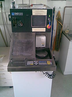
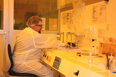
Due to high substrate costs for LiNbO3 and especially KTP we do not apply a full wafer technology. For LiNbO3 we use commercial 4” diameter Z-cut wafers of congruent melting composition (CLN). For KTP we are using significantly smaller Z-cut wafers of flux-grown crystal quality. The wafers are cut into slices using an automatic dicing saw (Fig. 1). Within our cleanroom facilities the samples have to pass a three step cleaning procedure, where organic and inorganic pollutants are removed (Fig.2)
After this, waveguides can be fabricated with our waveguide fabrication techniques for lithium niobate and KTP.


