Integrated Quantum Optics in CLN and KTP
The idea of Integrated Quantum Optics using nonlinear optical waveguide substrates is to combine active optical elements such as frequency converters, electro- and acousto-optical devices with passive elements (directional couplers, tapers, beam splitters, junctions etc.). Of course a sophisticated device design will monolithically integrate a number of such functionalities within a single optical waveguide chip, a so called integrated optical circuit (IOC).
As an example Fig. 1 shows a simple device, which contains a parametric down- converter (periodically poled area) and a directional coupler (S-bend WDM) in order to separate the generated photons spatially. It also consists of high quality end-face coatings to improve the overall conversion efficiency and to block the pump light. Thus, this basic building block for quantum networks contains three functionalities [1].
Waveguide sample preparation
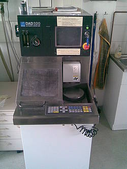
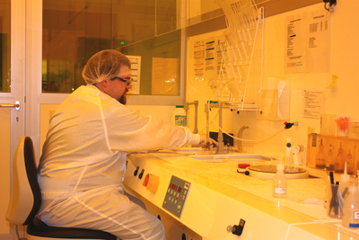
Due to high substrate costs for LiNbO3 and especially KTP we do not apply a full wafer technology. For LiNbO3 we use commercial 4” diameter Z-cut wafers of congruent melting composition (CLN). For KTP we are using significantly smaller Z-cut wafers of flux-grown crystal quality. The wafers are cut into slices using an automatic dicing saw (Fig. 2). Within our cleanroom facilities the samples have to pass a three step cleaning procedure, where organic and inorganic pollutants are removed.
⇒ Fabrication of waveguides in CLN
⇒ Fabrication of waveguides in KTP
⇒ Periodic poling
⇒ Device specific endface preparation
References
- An Efficient Integrated Two-Color Source for Heralded Single Photons
Stephan Krapick, Harald Herrmann, Viktor Quiring, Benjamin Brecht, Hubertus Suche, Christine Silberhorn
[PDF, New J. Physics 15, 033010 (2013)]


