
Quantum Devices
Future applications of optical quantum technologies depend to a large extent on the availability of miniaturised and reliable optical components with specially tailored functions. In our group, we are working on the development of so-called integrated optical circuits for various quantum applications. The aim is - analogous to integrated electrical circuits - to integrate various optical functional elements in a common substrate and thus realise optical chips with complex functionality, high efficiency and compact design.
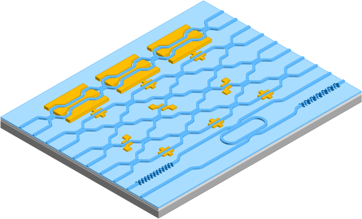
The "LiNbO3 toolbox" -- a development kit with functional elements
We utilise the properties of lithium niobate for our circuits. This is a dielectric crystal with excellent electro-optical and non-linear optical properties. Circuits are realised either in the substrate material with titanium-diffused waveguides or, more recently, primarily in thin-film lithium niobate (TFLN).
We have now developed a large number of different functional elements for both manufacturing technologies [1]. This provides us with a modular system of elements with which even more complex circuits can be monolithically integrated. This not only achieves a miniaturised structure, but also substantially increases stability, which is difficult to achieve with conventional optical structures, but is absolutely essential for the quantum experiment.
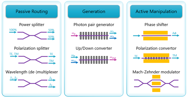
In addition to straight waveguides, the range of functional elements includes, for example, passive coupler structures for power splitting or as polarisation splitters and periodically poled elements for non-linear optical interactions such as frequency conversion or photon pair generation. Another category of functional elements are the electro-optical components, which can be used to manipulate light properties such as phase, power or polarisation with electrical control signals.
Photon pair sources
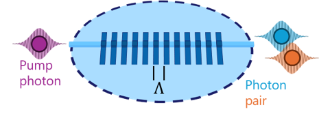
Sources for the generation of single photons or photon pairs are fundamental requirements for many quantum optical applications. In recent years, we have developed a variety of different integrated optical versions of such sources [2-4]. All of these sources utilise the chi(2) nonlinearity of LiNbO3, which enables the generation of photon pairs by parametric down-conversion (PDC). In this process, a pump photon decays into two daughter photons, known as the signalling and idler photon. This PDC process is subject to the rules of energy conservation and phase matching (momentum conservation), whereby the latter can be realised by quasi-phase matching in a periodically polarised structure.
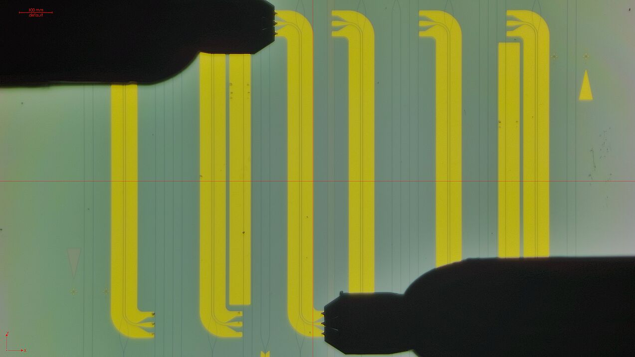
Work in recent years has focussed on the development of specific customised sources. These include, for example, user-friendly plug-and-play sources with fibre pigtails or spectrally narrow-band PDC sources that can be efficiently coupled to quantum memories, for example.
Future work will focus on the development of sources in TFLN. By utilising waveguide dispersion or resonant structures, for example, completely new design possibilities arise in TFLN with a wide range of applications in quantum computing, metrology and cryptography.
Electro-optical modulators
The electro-optical effect can be utilised in lithium niobate components to manipulate light properties. Ultra-fast modulators with bandwidths of several 10 GHz and low switching voltages can be realised with TFLN components. The phase of a light wave, for example, is changed via the electrical control signal. If this phase modulator is located in the arm of a Mach-Zehnder interferometer, this phase modulation causes intensity modulation at the output of the interferometer. In addition to phase and intensity, the polarisation of the light wave can also be changed, for example.
We are currently developing such electro-optical components in TFLN. The main aim is to develop components with properties specially adapted to the specific requirements of quantum optical applications.
Photonic circuits for quantum optical applications
The main goal of "integrated quantum optics" is the monolithic integration of complex optical systems into "optical chips" with specific functionality. Such miniaturisation, accompanied by simplified handling, significantly increased stability and low-cost fabrication, is essential to make optical quantum technologies suitable for everyday use.
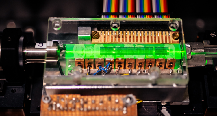
We have presented a "HOM chip" as an example of an integrated optical circuit for a typical quantum experiment [5]. On the chip, photon pairs are generated by a non-linear process. These are spatially separated and fed to different waveguides. Voltage signals applied to the electrodes of the chip cause a polarisation conversion and simultaneously enable a time delay between the photons. At the end of the chip, the two photons are then recombined in an (integrated optical) beam splitter. Quantum interference causes the so-called Hong-Ou-Mandel effect (HOM effect): If the photons reach the beam splitter at the same time and their properties are identical, they always leave the beam splitter as a pair. This is a fundamental quantum property of light and serves as the basis for many then much more complex quantum logic operations, e.g. in future quantum computers.
While the circuit described above was still realised with conventionally manufactured titanium monodiffusers, we are now increasingly working on circuits in TFLN. The significantly stronger waveguide should make it possible to realise even more compact circuits with higher integration densities.
Further reading
[1] P.R. Sharapova, et al, "Toolbox for the design of LiNbO3-based passive and active integrated quantum circuits", New J. Phys. 19, 123009 (2017) , DOI: 10.1088/1367-2630/aa9033
[2] N. Montaut, et al, "High-Efficiency Plug-and-Play Source of Heralded Single Photons", Physical Review Applied 8 024021 (2017), DOI: 10.1103/physrevapplied.8.024021
[3] K.H. Luo, H. Herrmann, S. Krapick, B. Brecht, R. Ricken, V. Quiring, H. Suche, W. Sohler, C. Silberhorn, "Direct generation of genuine single-longitudinal-mode narrowband photon pairs", New Journal of Physics, 073039 (2015), DOI: 10.1088/1367-2630/17/7/073039
[4] S. Babel, et al," Ultrabright, two-color photon pair source based on thin-film lithium niobate for bridging visible and telecom wavelengths" Optics Express 33, 52729 (2025), DOI: 10.1364/oe.571605
[5] K.-H. Luo, et al, "Nonlinear integrated quantum electro-optic circuits", Science Advances 5, eaat1451 (2019), DOI: 10.1126/sciadv.aat1451
Recent publications from the Quantum Devices group
Widely non-degenerate nonlinear frequency conversion in cryogenic titanium in-diffused lithium niobate waveguides
N.A. Lange, S. Lengeling, P. Mues, V. Quiring, W. Ridder, C. Eigner, H. Herrmann, C. Silberhorn, T. Bartley, Optics Express 33 (2025).
Harnessing temporal dispersion for integrated pump filtering in spontaneous heralded single-photon generation processes
J. Brockmeier, T. Schapeler, N.A. Lange, J.P. Höpker, H. Herrmann, C. Silberhorn, T. Bartley, New Journal of Physics (2025).
Photorefraction and in-situ optical cleaning in various types of LiNbO3 waveguides
M. Kirsch, C. Kießler, S. Lengeling, M. Stefszky, C. Eigner, H. Herrmann, C. Silberhorn, Optics & Laser Technology 193 (2025).
Ultrabright, two-color photon pair source based on thin-film lithium niobate for bridging visible and telecom wavelengths
S. Babel, L. Bollmers, F. Roeder, W. Ridder, C. Golla, R. Köthemann, B. Reineke, H. Herrmann, B. Brecht, C. Eigner, L. Padberg, C. Silberhorn, Optics Express 33 (2025).
SPDC single-photon source in Ti-indiffused diced ridge LiNbO3 waveguides
C. Kießler, M. Kirsch, S. Lengeling, H. Herrmann, C. Silberhorn, Optics Continuum 4 (2025).
Show all publications