Equipment: Specimen preparation for electron microscopy
Transmission electron microscopy (TEM) requires samples with a very small thickness down to few atomic layers in the area of interest. For the preparation of such specimens there are different preparation procedures:
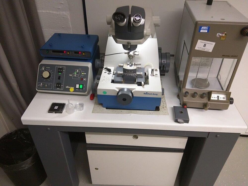
Cross-section preparation: By sawing the sample and gluing individual pieces a sandwich is created in which the sample surface and internal interfaces (in the case of thin film layer systems) point vertically down. For stability reasons this sandwich is fixed in a potty type of brass ring. The sample is then thinned mechanically down to 100 µm or less. Using a final Ar ion milling step the sample is then thinned down to electron transparency in the centre.
Plane-view preparation: This technique is very similar to cross-section preparation. Since the surface is to be looked at in top-view, one starts with ultrasonic drilling of a 3 mm disk of the material. This is followed by a thinning procedure as in cross-sectional preparation, but with all thinning steps only from the backside, to keep all structures on the original surface.
The techniques described above are well suited for hard and brittle materials, mostly with structures of interest near the surface. There is much experience with substrates of silicon, GaAs and sapphire. However, also other materials systems such as carbon fiber reinforced plastics have been prepared this way.
Wet-chemical plane-view preparation: a further option for the fast thinning of plane-view specimens of silicon is by the use of hydrofluoric jet-etching. A suitable apparatus for this is under construction.
Electrolytic thinning: metallic materials are prepared in collaboration with the Chair of Material Science at the Faculty of Mechanical Engineering by electrolytic etching and polishing.
TEM grids: This fast technique is suitable for small particles dispersed in suspensions or granular media. Here, a metallic grid out of Cu or Au, sometimes coated with a thin (10 nm), sometimes holey film of carbon is used. A suspension droplet is applied, leaving behind nanoparticles attached to the grid.
FIB preparation: the cross-sectional preparation of materials compounds and of selected sample areas is done using focused ion beam (FIB) machines in collaboration with the department of chemistry and other external partners.
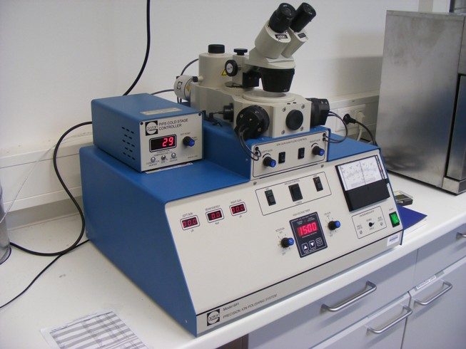
Ion beam etching apparatus Gatan PIPS Model 691
- Ion energy: 1.0 - 6.0 keV
- Ion beam inclination angle: -10° to +10°
- LN2 cooling
- Attachable light microscope
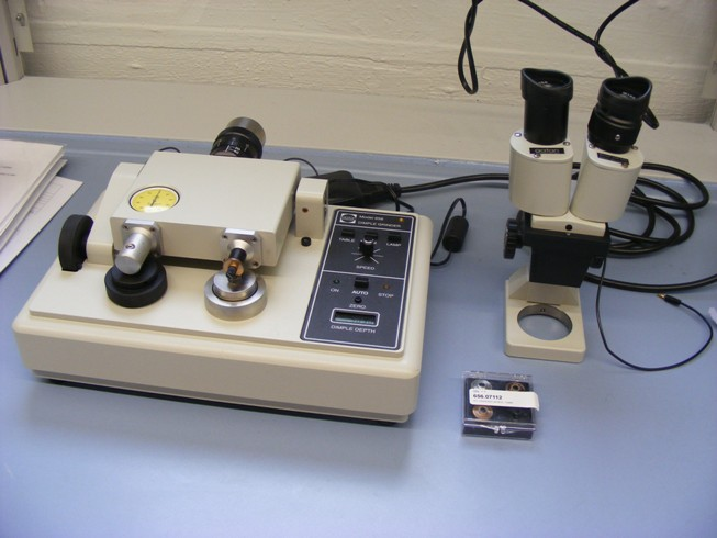
Dimple grinders: Gatan Model 656
- Rotation speed and bearing weight continuously adjustable
- Attachable light microscope
Grinding machine Bühler
- Angled grinding of silicon in optical quality
- Struers magnetic fixture system for grinding and polishing media

Grinding machine Jean Wirtz TE200
Thinning of brittle materials
- continuously adjustable rotation speed
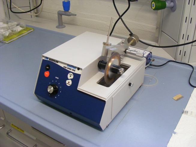
Scheibensäge Bühler IsoMet
- Niedriggeschwindigkeitssäge zum Zuschneiden von Proben
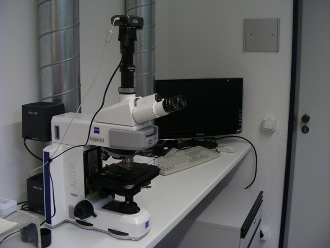
Light microscope Zeiss Axioscope
- Digital image acquisition system
- Reflection and transmission imaging
- differential interference contrast
Ultraschall-Kernbohrer
Ausbohren von Plan-view-Proben aus Halbleiterscheiben

Gatan Probenstanze
Ausstanzen metallischer Folien