Transmission electron microscopy
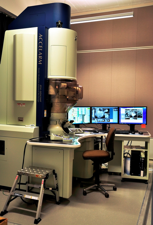
JEOL JEM-ARM200F: Cs-corrected highest resolution field emission TEM/STEM
- Acceleration voltage: 30 - 200 kV
- Cold field emitter
- Probe Cs corrector with aberration correction up to 5th order (CEOS ASCOR)
- TEM point resolution: 0.19 nm, information limit: 0.11 nm
- STEM point resolution: 0.08 nm at 200 kV, ≤ 0.20 nm at 30 kV
- Energy resolution ≤ 0.30 eV (FWHM ZLP)
- 4k x 4k CMOS camera (Gatan OneView)
- 2k x 2k CCD camera (Gatan UltraScan)
- STEM BF, ABF, DF and HAADF detectors
- 8-fold segmented STEM DF detector for differential phase contrast imaging
- Energy dispersive X-ray spectroscopy system with SDD detektor (JEOL)
- Post column energy filter for EELS, dual EELS and EFTEM (Gatan GIF Quantum ER)
- Single tilt, high tilt and analytic double tilt specimen holders
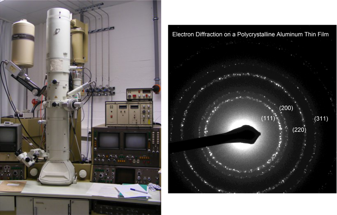
Jeol JEM-2000FX
- Acceleration voltage: 80 - 200 kV
- Thermionic electron source (currently tungsten)
- Point resolution ~0.3 nm
- Specimen holder: Single tilt holder, 2 specimens, max. tilt +/- 30°
- Energy dispersive X-ray spectroscopy system: EDAX with Be window
- FastScan CCD camera (TVIPS)
Scanning electron microscopy
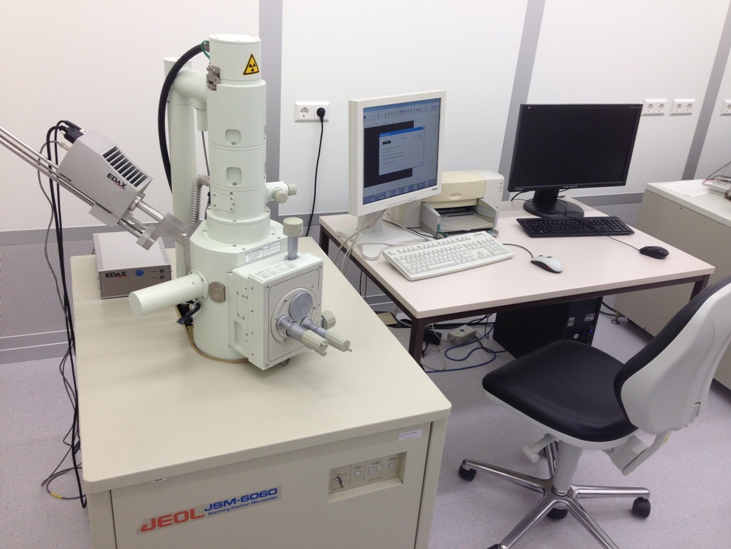
Jeol JSM-6060
- Tungsten hairneedle emitter
- Acceleration voltage: 0.2 - 30 kV
- Detector for secondary electrons
- EDAX-EDX for elemental analysis with Si drift detector (SDD) for elements above atomic number 5
- 131 eV resolution
- point measurement; linescan; mapping
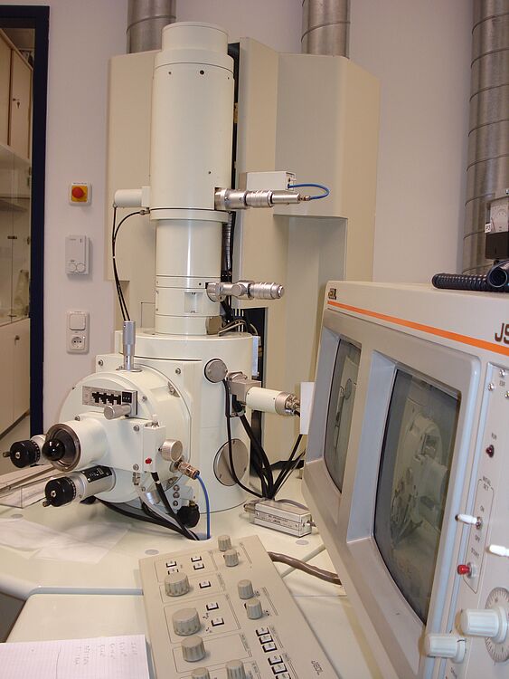
Jeol JSM-6300F
- Field emitter
- Acceleration voltage: 0.2 - 30 kV
- Detectors for secondary and backscattered electrons
- Point Electronic scan control and data acquisition unit
Scanning probe microscopy
Digital Instruments: Dimension 3100
- Sample size 150 mm x 12 mm
- Stage movement x, y 150 mm with 2 µm resolution
- Video optics with zoom 150-675 µm viewing area
- Piezo scan head range; 90 µm in x, y and 6 µm in z
- 16 bits DAC giving sub nanometer resolution
- Max. 512 x 512 samples/image
- Contact and tapping mode AFM
- Conductivity mapping
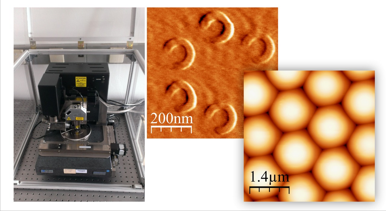
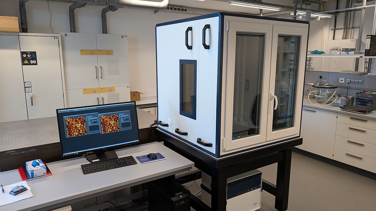
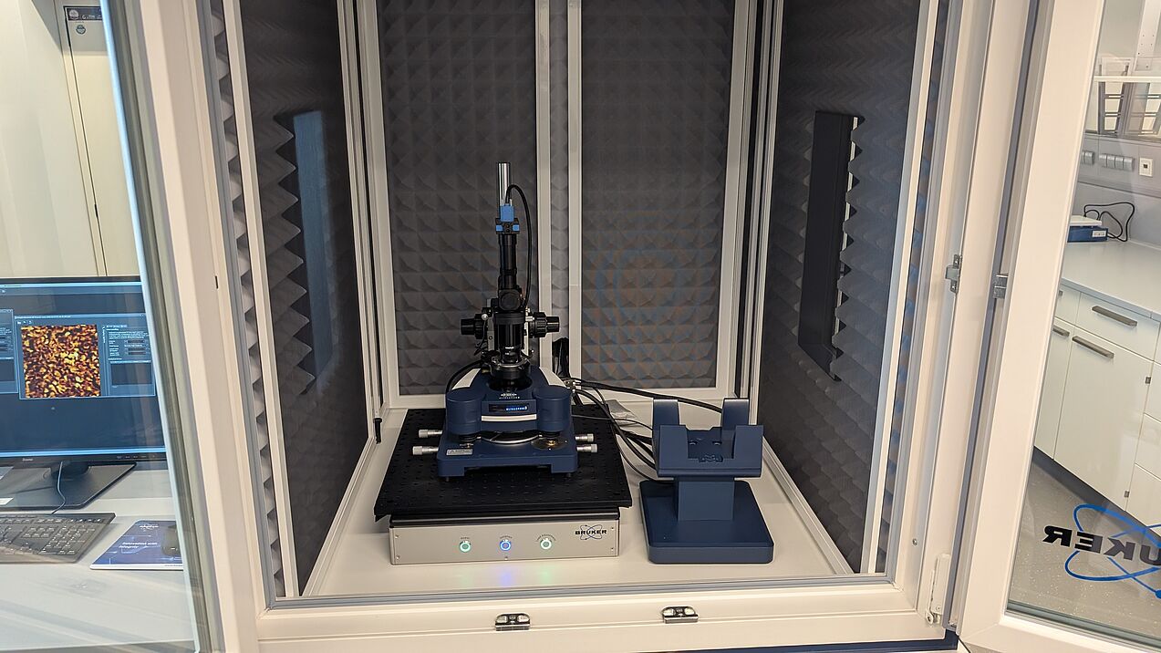
Bruker NanoWizard ULTRA Speed 3
- Messmodi: Kontaktmodus, Tapping-Modus, Forcemapping, erweiterte Spektroskopiemodi (inkl. verschiedener Force-Clamp-Modi und Rampen-Designs), MFM, EFM, elektrochemische Messungen sowie rasternde elektrochemische Mikroskopie (SECM)Scan-Geschwindigkeit: bis zu 1400 Linien/Sekunde in Flüssigkeit
- Piezorasterkopf: Verfahrbereich 30 µm in x und y, 6,5 µm in z
- Verfahrbereich des Probentisches: 20 × 20 mm²
- Maximale Probenhöhe: bis zu 140 mm
- Maximale Bildauflösung: bis zu 8192 × 8192 Pixel
- Atomare Auflösung im geschlossenen Regelkreisbetrieb
- Stretching-Stage (In-situ mechanische Prüfungen):
- Kraftbereich: 10 N bis 10.000 N
- Verfahrgeschwindigkeit: 0,006 bis 3 mm/min
- Maximaler Verfahrweg: 40 mm für Proben mit 5 mm Länge zwischen den Klemmbacken (Auflösung: 100 nm)