UPB Bildmarke
Nanopatterning - Nanoanalysis - Photonic Materials
Contact
  • Deutsch
  • English
    • Open Page "Research"
    • TEM,STEM
    • EELS
      • Open Page "Photonic materials"
      • Perovskite nanocrystals
      • Heteroepitaxial structures
      • Plasmonic structures
      • Left-hand materials
      • Open Page "Nano structure"
      • Block copolymer lithgraphy
      • Soft lithography with PDMS
      • Metal-assisted wet-chemical etching
  • Publications
  • Team
  • Teaching
  • Theses
    • Open Page "Equipment"
    • Nanopatterning
    • Material deposition and removal
    • Microscopy and Spectroscopy
    • Specimen preparation for electron microscopy
    • Magnetic resonance spectroscopy
    • Optical and electrical characterization
  • News
  • Events
  • Imagefilm
  • Contact
Important Links
  • Home
  • Research
  • Publications
  • Teaching
  • Team
  • Theses
  • Equipment
  • News
  • Events
  • Contact
Nano struc­ture
Nano struc­ture
Nanoana­lys­is
Photon­ic ma­ter­i­als
  1. Faculty of Science
  2. Department of Physics
  3. Nanopatterning, Nanoanalysis, Photonic Materials
  4. Research

Nano struc­ture

Δ Nanoshpere lithography
Δ Block copolymer lithography
Δ Soft lithography with PDMS

Nanoana­lys­is

Microscopy
Δ Light microscopy
Δ Scanning electron microscopy (SEM)
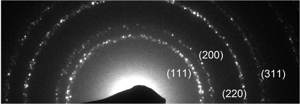
Δ Transmission and scanning transmission electron microscopy (TEM,STEM, SAED, HRTEM, EFTEM)
Δ Scanning probe microscopy (SPM)
Δ Atomic force, scanning tunneling and magnetic force microscopy
Δ Microreflectometry
Δ Nanomask analysis

Spectroscopy
Δ Spectroscopy in the electron microscope
  - Energy-dispersive X-ray spectroscopy (EDXS)
  - Electron Energy-Loss Spectroscopy (EELS) 
Δ Photoemission spectroscopy (XPS/ESCA)
Δ Spectral response of solar cells
Δ Fourier transform infrared spectroscopy (FTIR)
Δ Photoluminescence spectroscopy (PL)
Δ Electron spin resonance (ESR)
Δ Optically detected electron spin resonance (ODMR)
Δ Optical and electrical surface analysis

Photon­ic ma­ter­i­als

Different materials are analyzed, which are relevant for modern applications in optoelectronics and photonics:

Δ Perovskite nanocrystals
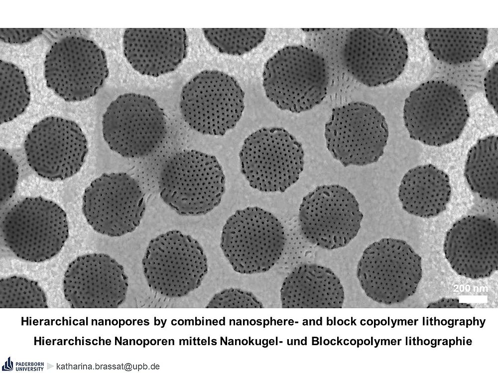
Δ Heteroepitaxial structures (SiC/Si, GaN/SiC, GaAs/InAs)
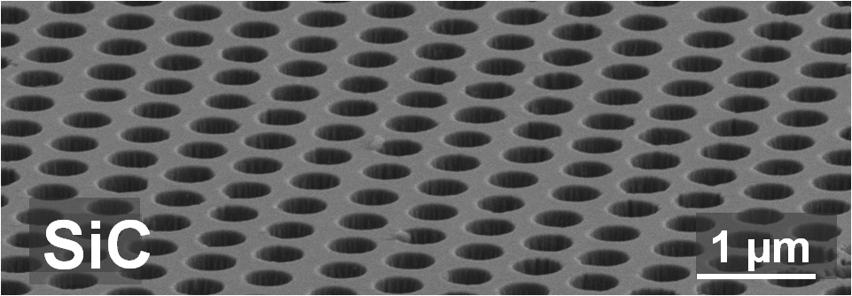
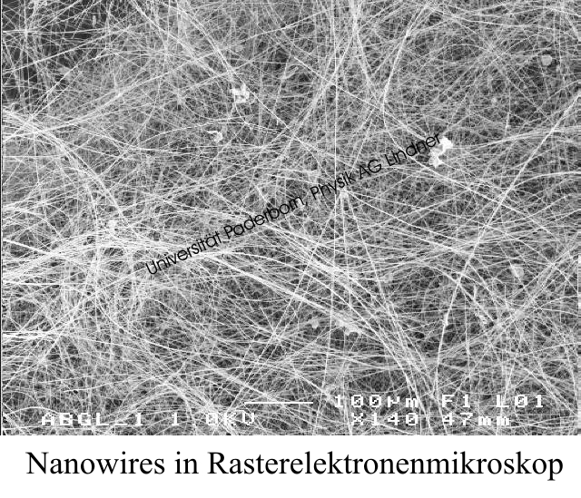
Δ SiC nanowires and composites
Δ ZnO nanowires
Δ Lattice defects in Si, GaN, GaAs
Δ Doped LiNbO3
Δ Plasmonic structures
Δ Left-hand materials

Nanopatterning - Nanoanalysis - Photonic Materials

Learn more about us:

TEM,STEM EELS Photonic materials Nano structure

Nanopatterning - Nanoanalysis - Photonic Materials

Warburger Str. 100
33098 Paderborn
Germany

Quick links
  • Paderborn University
  • Faculty of Mechanical Engineering
  • Faculty of Computer Science, Electrical Engineering and Mathematics
  • Faculty of Business Administration and Economics
  • Faculty of Science
  • Faculty of Arts and Humanities
Universität Paderborn

Warburger Str. 100
33098 Paderborn
Germany

Phone University

+49 5251 60-0
Legal notice
  • Imprint
  • Data privacy
  • Whistleblower system
Social networks