Welcome!
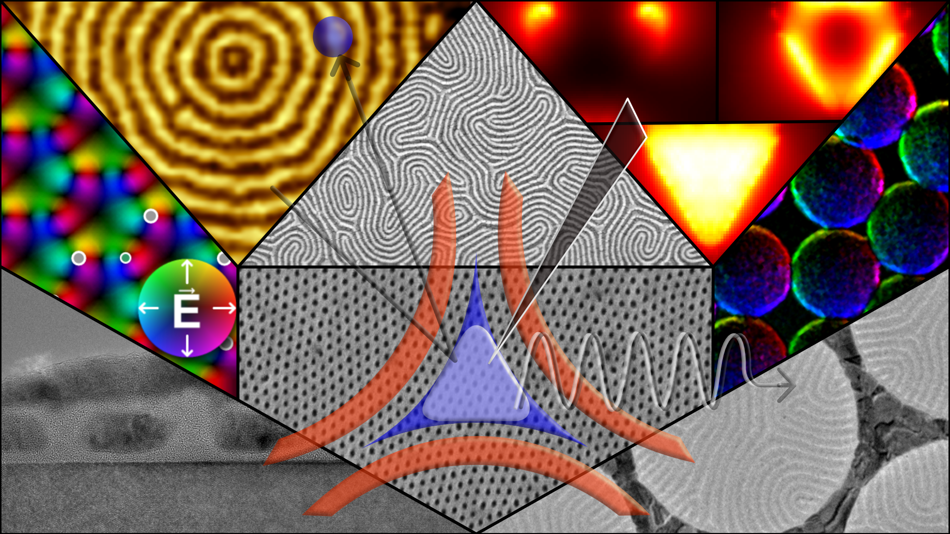
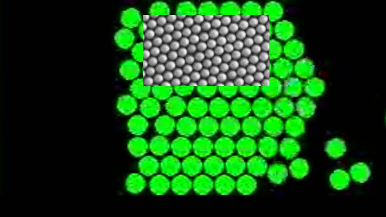
The Nanostructuring - Nanoanalysis - Photonic Materials group is concerned with the production of new optoelectronic and photonic materials, the development of the nanostructuring methods required for this and the precise analysis of their properties. In terms of structuring methods, the focus is on cost-effective processes such as self-organising nanoball lithography (structure sizes 500 - 50 nm) and block copolymer lithography (structure sizes down to < 10 nm). Highly spatially resolved electron microscopic and spectroscopic methods are used to characterise nanoscale materials. Pioneering new measurement methods such as STEM-DPC for analysing atomic electric fields and modern methods of data evaluation are being further developed. The overarching aim is to understand the physical mechanisms that occur during the production and structuring of materials in detail and to correlate them with the material properties.
Veranstaltungen
Publications
2025
An applied noise model for scintillation-based CCD detectors in transmission electron microscopy
C. Zietlow, J.K.N. Lindner, Scientific Reports 15 (2025).
An applied noise model for low-loss EELS maps
J.K.N. Lindner, C. Zietlow, Ultramicroscopy (2025).
An applied noise model for low-loss EELS maps
C. Zietlow, J. Lindner, Ultramicroscopy 270 (2025).
An applied noise model for scintillation-based CCD detectors in transmission electron microscopy.
C. Zietlow, J. Lindner, Sci Rep 15 (2025) 3815.
An unbiased ADMM-TGV algorithm for the deconvolution of STEM-EELS maps
C. Zietlow, J. Lindner, Ultramicroscopy (2025).
Show all publications