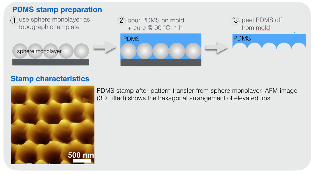
Metal-assisted wet-chemical etching (MACE)
Discovered in 2000, metal-assisted wet-chemical etching (MACE) has developed into a method for fabrication of nanostructured semiconductor surfaces (e.g. Si), in particular of ultrahigh-aspect-ratio nanostructures, by transferring a 2D nanopattern into the third dimension [1,2]. It relies on the catalyzing action of a noble metal (like Au, Pt and Ag) deposited on the semiconductor in contact with an oxidizing etch solution (e.g. H2O2) to generate holes. This leads (i) to local oxidation and dissolution of the semiconductor beneath the metal and (ii) to hydrogen reduction to H2 gas. Consequently, the metal-covered areas sink down during the etching, thus transferring the mask pattern into the semiconductor. By employing masks prepared by nanosphere lithography, ordered nanopillar and nanohole arrays can be obtained, of interest e.g. for photonic crystals with tailored optical i.e. anti-reflective and light trapping properties [3].
Apart from vertical also conical geometries can be realized by means of increased H2O2 concentration or light irradiation, which raises the hole production rate above the rate of Si dissolution beneath the metal. Hence, holes are not completely consumed and migrate towards areas not covered by metal, where they induce lateral etching.
By intentionally changing the H2O2/HF ratio of the solution during etching, nanopillars with alternating diameter become feasible, including nanopillars with single and multiple constrictions, attractive for high-efficiency thermoelectric generators [3].
Furthermore, advanced 3D shaping capabilities of MACE, which result in spiral and hinged nanostructures, are enabled by the lateral motion and by folding of tailored catalyst film geometries, respectively [4,5].
[1] X. Li, P. W. Bohn: Appl. Phys. Lett. 77 (2000) 2572.
[2] F. Toor et al.: Nanotechnol. 27 (2016) 412003.
[3] M. Kismann, T. Riedl, J. K. N. Lindner: Mater. Sci. Semicond. Process. 128 (2021) 105746.
[4] O. J. Hildreth, A. G. Fedorov, C. P. Wong: ACS Nano 6 (2012) 10004.
[5] K. Rykaczewski et al.: Nano Lett. 11 (2011) 2369.