
Publication in Nature Chemistry
In collaboration with colleagues from the University of Münster, the Technische Universität Berlin and the Tor Vergata University of Rome in Italy, physicists from Paderborn University have succeeded in depositing ultra-thin organic layers on the semiconductor material silicon with atomic precision. This adds a wide range of new possibilities to the field of silicon-based semiconductor technology which is used in microelectronics and many other applications, including, for example, the absorption and generation of light or for sensors. The breakthrough was achieved by combining specially prepared silicon surfaces with small reactive organic ring molecules, known as N-heterocyclic carbenes. These are molecules with a divalent carbon. The new hybrid material could, for instance, be used to produce more efficient solar cells in the future. The scientists' findings have now been published in the renowned journal Nature Chemistry.
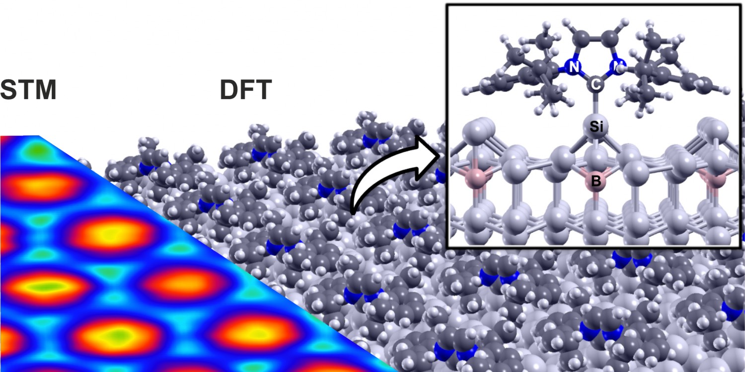
Organic electronics has conquered the mass market thanks to powerful applications such as flexible, high-contrast displays, new batteries, and storage media. In addition, layers of organic molecules offer great potential for more efficient renewable power generation. In photovoltaics, however, semiconductors are mostly made of silicon: “Extending advanced silicon technology to include the diverse applications of organic electronics requires organic molecules to be anchored to the silicon surface as precisely as possible. However, since both the organic molecules and the silicon surfaces have a large number of different bonding sites, organic layers on silicon have so far generally consisted of a disordered mixture of differently bound and differently oriented molecules. Due to this, these layers contain numerous defects that inhibit the transport of electrons through the organic-inorganic interfaces and make technical applications difficult,” explains Prof. Dr. Wolf Gero Schmidt, Chair of Theoretical Materials Physics at Paderborn University.
Together with chemists from Münster and physicists from Berlin and Rome, the Paderborn-based physicists Dr. Hazem Aldahhak and Dr. Uwe Gerstmann from Prof. Schmidt's working group have found a way to deposit high-order and defect-free organic layers on silicon. To do so, they combined specially prepared silicon surfaces with a particularly versatile class of organic molecules. “By partially replacing tetravalent silicon atoms with trivalent boron below the substrate surface, we were able to specifically reduce the surface’s reactivity,” Schmidt explains. And Dr. Aldahhak adds, “We also take advantage of the special bonding configuration of carbenes. Carbenes contain a carbon atom with only two bonds instead of the usual four. Instead of the 'missing' bonds, they have a pair of electrons which they use to dock directly onto the surface, forming a perfectly ordered molecular layer on the semiconductor,” Aldahhak continues. The atomic precision of the bonding between organic and inorganic materials results in interfaces of exceptional quality, such as those required for solar cells with a high quantum yield.
For publication: https://www.nature.com/articles/s41557-021-00721-2
Prof. Dr. Wolf Gero Schmidt; Nina Reckendorf, Press, Communications and Marketing Office
To the press release of the University of Münster: New method for molecular functionalization of surfaces (uni-muenster.de)


